DIP-switches and buttons information
The MSE-Embedded platform contains one 8-position DIP-switche and twelve buttons as shown in the below figure.
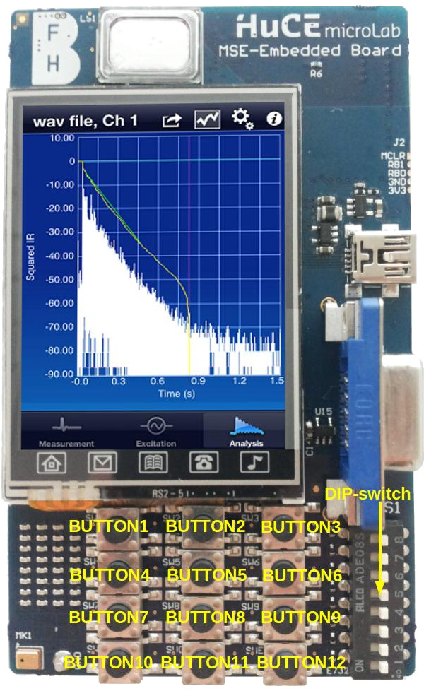
Each of these switches and buttons is connected to an individual FPGA-pin. In case a switch is activated it gives 0V (logic 1) and if it is not activated it gives VCC (logic 0) on the FPGA-pin (the switches are therefore active low). Furthermore, all switches do not include a debouncing circuit and are connected to clock-inputs of the FPGA.
DIP-switch(es) information
The below table indicates at which FPGA-pin each of the switches of the DIP-switches is connected. And here you find an example tcl script that can be used for pin-assignment in Quartus.
| Switch | 1 | 2 | 3 | 4 | 5 | 6 | 7 | 8 |
|---|---|---|---|---|---|---|---|---|
| DIP-switch | PIN_B11 | PIN_A11 | PIN_B12 | PIN_A12 | PIN_AA12 | PIN_AB12 | PIN_AA11 | PIN_AB11 |
Button(s) information
The below table indicates at which FPGA-pin each of the buttons is connected. And here you find an example tcl script that can be used for pin-assignment in Quartus.
| BUTTON1 | BUTTON2 | BUTTON3 |
|---|---|---|
| PIN_H11 | PIN_H10 | PIN_G11 |
| BUTTON4 | BUTTON5 | BUTTON6 |
| PIN_G10 | PIN_G9 | PIN_G8 |
| BUTTON7 | BUTTON8 | BUTTON9 |
| PIN_G7 | PIN_F7 | PIN_E10 |
| BUTTON10 | BUTTON11 | BUTTON12 |
| PIN_E9 | PIN_D7 | PIN_D6 |